Hoodi, Bangalore, Karnataka
- GST NO. : 29AABCU9740P1ZH
View Mobile Number
50 Piece (MOQ)
| Business Type | Manufacturer, Exporter, Supplier |
| Growth method | CVD synthesis |
| Appearance (color) | Transparent |
| Transparency | > 97% |
| Click to view more | |
Product Details
Processed in Clean Room Class 1000
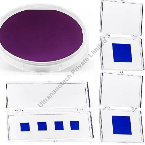
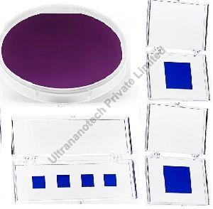
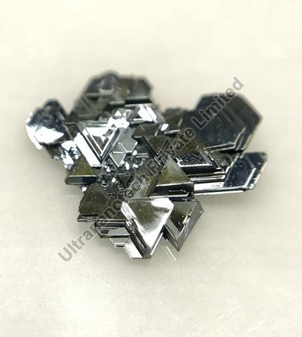
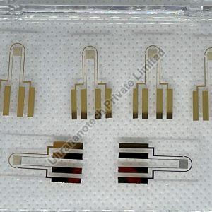
Our monolayer graphene on SiO₂/Si (fully covered) is a bidimensional material produced by CVD and transferred to a circular substrate of SiO₂/Si (300nm) by a wet transfer process. We consider it to be a benchmark product in the graphene market – not only for its excellent quality, but also for its shape, size and number of applications.”
FET Electron Mobility on Al2O3 passivated SiO2/Si: 6900 cm2 /Vs (doi: http://dx.doi.org/10.1063/1.4972847)
FET Electron Mobility on SiO₂/Si: 3760 cm2/Vs DOI: https://doi.org/10.1103/PhysRevLett.119.066802
Looking for "Monolayer Graphene on SiO₂/Si 300 nm" ?
Explore More Products
Our Blogs


