Hoodi, Bangalore, Karnataka
- GST NO. : 29AABCU9740P1ZH
View Mobile Number
Sensing Device
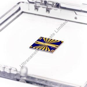
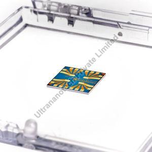
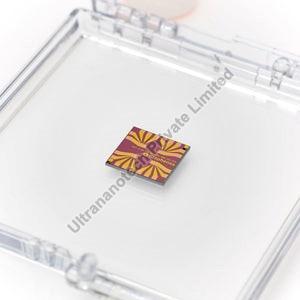
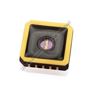
Leading Manufacturers, Exporters, Wholesaler, Distributor and Trader of GFET-S10 for Sensing applications, GFET-S11 for Sensing Applications, GFET-S12 for Sensing Applications, GFET-S20 for Sensing Applications, GFET-S20P for Sensing Applications, GFET-S22 for Sensing Applications, GFET-S22P for Sensing Applications and MGFET-4D for Sensing Applications from Bangalore.
| Business Type | Manufacturer, Exporter, Supplier |
| Brand Name | Ultrananotech |
| Condition | New |
| Application | Industrial, Laboratory |
| Feature | High Quality, Long Life |
| Country of Origin | India |
TYPICAL SPECIFICATIONS
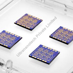
- GFET-S10 (Die size 10 mm x 10 mm)
- Processed in Clean Room Class 1000
- Growth method: CVD synthesis
- Polymer assisted transfer
- Chip dimensions: 10 mm x 10 mm
- Chip thickness: 675 μm
- Number of GFETs per chip: 36
- Gate oxide thickness: 90 nm
- Gate oxide material: SiO2
- Dielectric Constant of the SiO2 layer: 3.9
- Resistivity of substrate: 1-10 Ω.cm
| Business Type | Manufacturer, Exporter, Supplier |
| Brand Name | Utrananotech |
| Condition | New |
| Application | Industrial, Laboratory |
| Feature | Durable, High Quality, Long Life |
| Country of Origin | India |
FEATURES
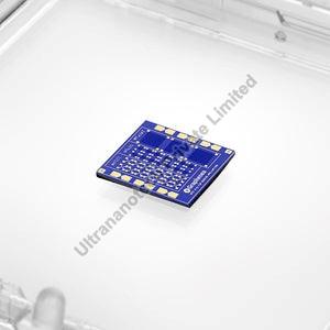
- Growth method: CVD synthesis
- Polymer assisted transfer
- Chip dimensions: 10 mm x 10 mm
- Chip thickness: 675 μm
- Number of GFETs per chip: 31
- Gate oxide thickness: 90 nm
- Gate oxide material: SiO2
- Dielectric Constant of the SiO2 layer: 3.9
- Resistivity of substrate: 1-10 Ω.cm
- Metallization: Au contacts
- Graphene field-effect mobility: >1000 cm2/V.s
- Dirac point: <50 V
- Minimum working devices: >75 %
| Business Type | Manufacturer, Exporter, Supplier |
| Brand Name | Ultrananotech |
| Condition | New |
| Application | Industrial, Laboratory |
| Feature | Durable, High Quality, Long Life |
| Country of Origin | India |
FEATURES
- Growth method: CVD synthesis
- Polymer assisted transfer
- Chip dimensions: 10 mm x 10 mm
- Chip thickness: 675 μm
- Number of GFETs per chip: 27
- Gate oxide thickness: 90 nm
- Gate oxide material: SiO2
- Dielectric Constant of the SiO2 layer: 3.9
- Resistivity of substrate: 1-10 Ω.cm
- Metallization: Au contacts
- Graphene field-effect mobility: >1000 cm2/V.s
- Dirac point: <50 V
- Minimum working devices: >75 %
| Business Type | Manufacturer, Exporter, Supplier |
| Brand Name | Ultrananotech |
| Condition | New |
| Application | Industrial, Laboratory |
| Feature | Durable, High Quality, Long Life |
| Country of Origin | India |
FEATURE
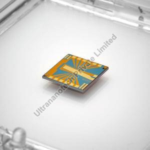
- GFET-S20 (Die size 10 mm x 10 mm)
- Processed in Clean Room Class 1000
- Growth method: CVD synthesis
- Polymer assisted transfer
- Chip dimensions: 10 mm x 10 mm
- Chip thickness: 675 μm
- Number of GFETs per chip: 12
- Gate oxide thickness: 90 nm
- Gate oxide material: SiO2
- Resistivity of substrate: 1-10 Ω.cm
| Business Type | Manufacturer, Exporter, Supplier |
| Brand Name | Ultrananotech |
| Condition | New |
| Application | Industrial, Laboratory |
| Feature | Durable, High Quality, Long Life |
| Country of Origin | India |
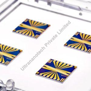
FEATURES
- Growth method: CVD synthesis
- Polymer assisted transfer
- Chip dimensions: 10 mm x 10 mm
- Chip thickness: 525 μm
- Number of GFETs per chip: 12
- Gate oxide thickness: 90 nm
- Gate oxide material: SiO2
- Resistivity of substrate: 1-10 Ω.cm
- Metallization: Au contacts
- Graphene field-effect mobility: >1000 cm2/V.s
- Encapsulation: ≈200 nm glutarimide-based
- Dirac point (liquid gating): <1V
- Minimum working devices: >75 %
| Business Type | Manufacturer, Exporter, Supplier |
| Brand Name | Ultrananotech |
| Condition | New |
| Application | Industrial, Laboratory |
| Feature | Durable, High Quality, Long Life |
| Country of Origin | India |
FEATURE
- Growth method: CVD synthesis
- Polymer assisted transfer
- Chip dimensions: 10 mm x 10 mm
- Chip thickness: 675 μm
- Number of GFETs per chip: 12 in parallel
- Gate oxide thickness: 90 nm
- Gate oxide material: SiO2
- Resistivity of substrate: 1-10 Ω.cm
- Metallization: Au contacts
- Graphene field-effect mobility: >1000 cm2/V.s
- Encapsulation: 50 nm Al2O3
- Dirac point (liquid gating): <1V
- Minimum working devices: >75 %
| Business Type | Manufacturer, Exporter, Supplier |
| Brand Name | Ultrananotech |
| Condition | New |
| Application | Industrial, Laboratory |
| Feature | Durable, High Quality |
| Country of Origin | India |
| Business Type | Manufacturer, Exporter, Supplier |
| Brand Name | Ultrananotech |
| Condition | New |
| Application | Industrial, Laboratory |
| Feature | Durable, High Quality, Long Life |
| Country of Origin | India |


