Hoodi, Bangalore, Karnataka
- GST NO. : 29AABCU9740P1ZH
View Mobile Number
CVD Graphene on Substrate
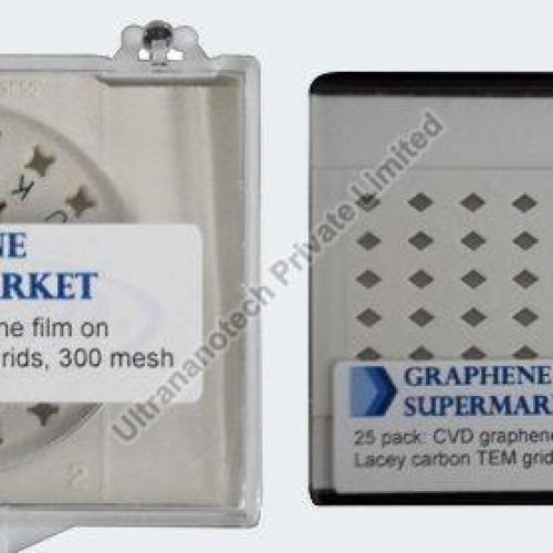
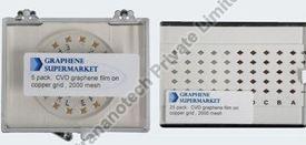
Leading Manufacturers, Exporters, Wholesaler, Distributor and Trader of CVD Graphene TEM Grids, Graphene on Copper 2000 TEM Grids, Monolayer Graphene on Cu with PMMA Coating, Monolayer Graphene on SiO₂/Si 300 nm and Monolayer Graphene on SiO₂/Si 90 nm from Bangalore.
| Business Type | Manufacturer, Exporter, Supplier |
| Packaging Size | 5 Pack |
| Thickness of CVD Graphene film | 0.3-2 nm (1-6 monolayers) |
| Typical Graphene Coverage | 60-90% |
| Brand Name | Graphene Supermarket |
Ultrathin CVD Graphene grids provide the ideal specimen support to achieve high resolution data in TEM imaging making them an ideal choice many TEM applications such as:
CVD Graphene grids can be used for the applications:
- Imaging of nanoparticles, proteins, viruses, DNA
- Medical Diagnostics
- Single Cell Studies
- 3D protein imaging
- Drug design
- Imaging of Biological Markers and bio-inspired nanomaterials
- Cryo-transmission electron microscopy, Electron Cryomicroscopy
- Single Particle Analysis ( SPA )
- Materials science and Semiconductor Researc
- Electron Energy Loss Spectroscopy (EELS)
| Business Type | Manufacturer, Exporter, Supplier |
| Brand Name | Graphene |
| Thickness of CVD Graphene film | 0.3-2 nm (1-6 monolayers) |
| Typical Graphene Coverage | 60-90%” |
| Available Size | 5 Pack, 25 Pack |
| Color | Grey |
Ultrathin CVD Graphene grids provide the ideal specimen support to achieve high resolution data in TEM imaging making them an ideal choice many TEM applications such as:
CVD Graphene grids can be used for the applications:
- Imaging of nanoparticles, proteins, viruses, DNA
- Medical Diagnostics
- Single Cell Studies
- 3D protein imaging
- Drug design
- Imaging of Biological Markers and bio-inspired nanomaterials
- Cryo-transmission electron microscopy, Electron Cryomicroscopy
- Single Particle Analysis ( SPA )
- Materials science and Semiconductor Research
- Electron Energy Loss Spectroscopy (EELS)
| Business Type | Manufacturer, Exporter, Supplier |
| Growth Method | CVD synthesis |
| Appearance (color) | Transparent |
| Transparency | > 97% |
| Coverage | > 98% |
| Number of graphene layers | 1 |
| Thickness (theoretical) | 0.345 nm |
| Sheet Resistance on SiO2/Si | 450±40 Ohms/sq (1cm x1cm) |
| Grain size | Up to 20 μm |
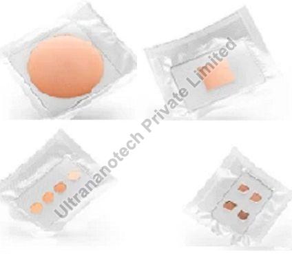
Monolayer Graphene on Cu with PMMA Coating – Processed in Clean Room Class 1000
A single-layer graphene film on a copper substrate. This product is provided with a PMMA coating on top of the Graphene in order ease the transfer process and to avoid contamination. It’s a high quality product, with a great homogeneity, and it is ideal for R&D departments and universities.
FET Electron Mobility on Al2O3 passivated SiO2/Si: 6900 cm2 /Vs (doi: http://dx.doi.org/10.1063/1.4972847)
FET Electron Mobility on SiO2/Si: 3760 cm2/Vs DOI: https://doi.org/10.1103/PhysRevLett.119.066802
Available Sizes:
- 6” Wafer
- 4” Wafer
- 60 mm x 40 mm
- 10 mm x 10 mm – Pack of 4
- 12 mm Circular – Pack of 4
- 1 inch x 1 inch
| Business Type | Manufacturer, Exporter, Supplier |
| Growth method | CVD synthesis |
| Appearance (color) | Transparent |
| Transparency | > 97% |
| Coverage | > 95% |
| Number of graphene layers | 1 |
| Thickness (theoretical) | 0.345 nm |
| Sheet Resistance on SiO₂/Si | 450±40 Ohms/sq (1cm x1cm) |
| Grain size | Up to 20 μm |
Processed in Clean Room Class 1000
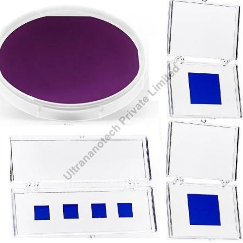
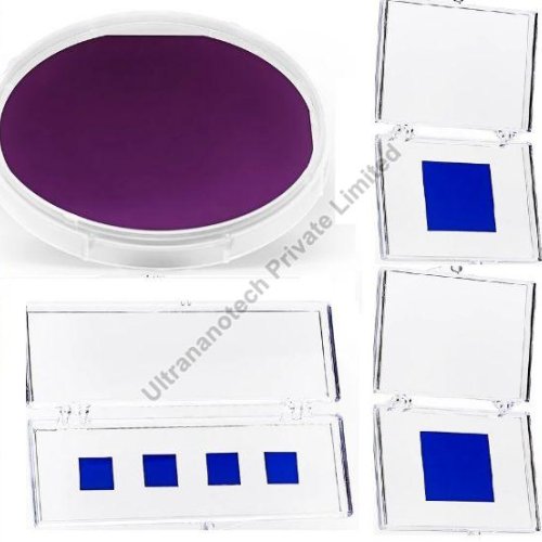
Our monolayer graphene on SiO₂/Si (fully covered) is a bidimensional material produced by CVD and transferred to a circular substrate of SiO₂/Si (300nm) by a wet transfer process. We consider it to be a benchmark product in the graphene market – not only for its excellent quality, but also for its shape, size and number of applications.”
FET Electron Mobility on Al2O3 passivated SiO2/Si: 6900 cm2 /Vs (doi: http://dx.doi.org/10.1063/1.4972847)
FET Electron Mobility on SiO₂/Si: 3760 cm2/Vs DOI: https://doi.org/10.1103/PhysRevLett.119.066802
| Business Type | Manufacturer, Exporter, Supplier |
| Growth Method | CVD synthesis |
| Appearance (color) | Transparent |
| Transparency | > 97% |
| Coverage | > 98% |
| Number of Graphene Layers | 1 |
| Thickness (theoretical) | 0.345 nm |
| Sheet Resistance on SiO₂/Si | 450±40 Ohms/sq (1cm x1cm) |
| Grain size | Up to 20 μm |
Our monolayer graphene on SiO₂/Si (fully covered) is a bidimensional material produced by CVD and transferred to a circular substrate of SiO₂/Si (90nm) by a wet transfer process. We consider it to be a benchmark product in the graphene market – not only for its excellent quality, but also for its shape, size and number of applications.”
FET Electron Mobility on Al2O3 passivated SiO2/Si: 6900 cm2 /Vs (doi: http://dx.doi.org/10.1063/1.4972847)
FET Electron Mobility on SiO₂/Si: 3760 cm2/Vs DOI: https://doi.org/10.1103/PhysRevLett.119.066802
Available Sizes:
- 6” Wafer
- 4” Wafer
- 10 mm x 10 mm
- 10 mm x 10 mm – Pack of 4
- 1 inch x 1 inch


